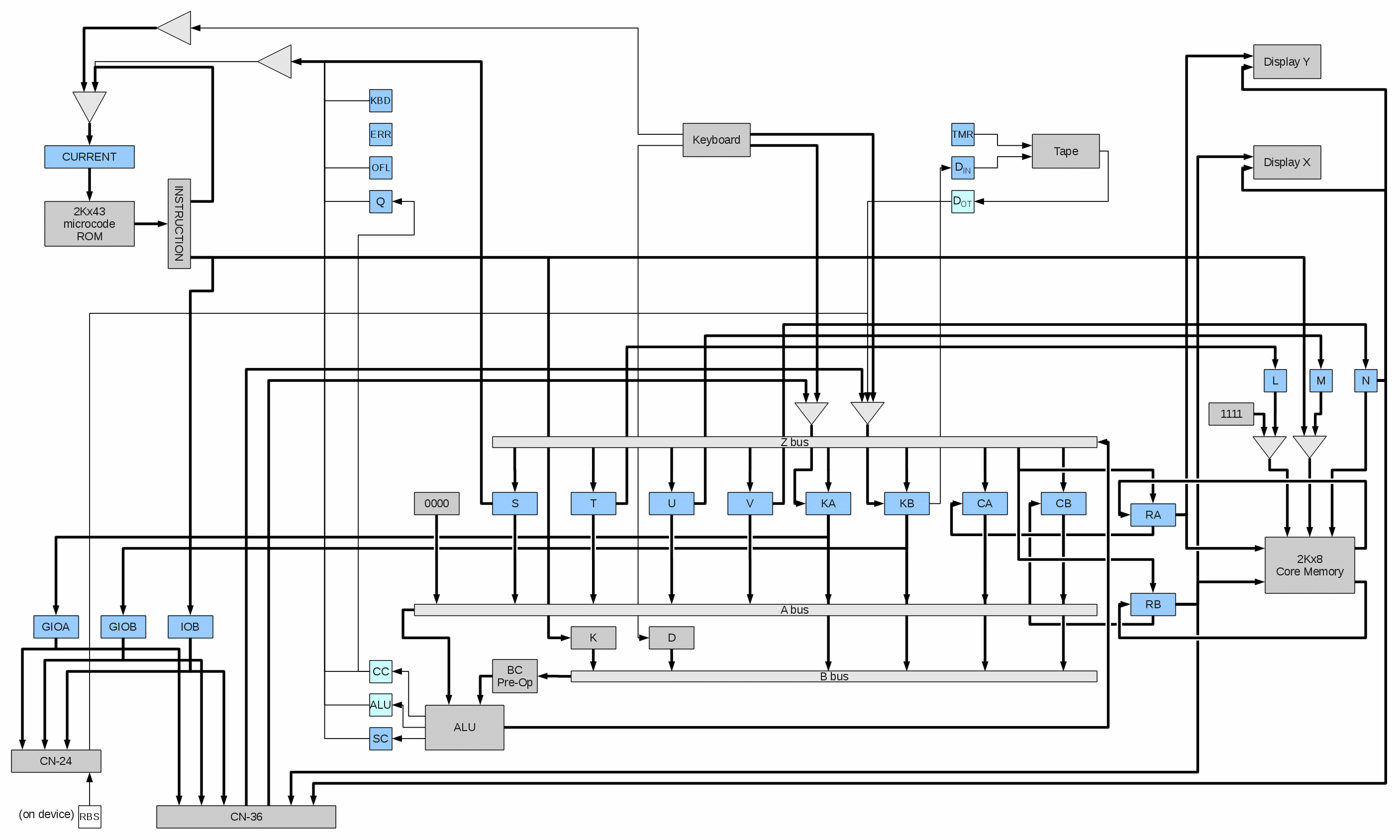
In the above diagram, fine lines represent single-bit (and serial) data paths,
while thicker lines represent multiple bits of data in parallel (typically 4).
Note, the hardware implements both parallel and serial paths,
depending on registers and access operations.
Hardware Registers
The registers in the block diagram are explained here:
| Reg Name | Num Bits | Access | Meaning/Use | |
|---|---|---|---|---|
| S | 4 | R/W | Machine State * | |
| T | 4 | R/W | Memory Address, Hi * | |
| U | 4 | R/W | Memory Address, Mid * | |
| V | 4 | R/W | Memory Address, Lo * | |
| KA | 4 | R/W | Input Data, Hi * | |
| KB | 4 | R/W | Input Data, Lo * | |
| CA | 4 | R/W | General Data, Hi * | |
| CB | 4 | R/W | General Data, Lo * | |
| GIOA | 4 | W/O | Expansion Output, Hi | |
| GIOB | 4 | W/O | Expansion Output, Lo | |
| IOB | 3 | W/O | Expansion Select | |
| L | 4 | n/a | Current Memory Address, Hi | |
| M | 4 | n/a | Current Memory Address, Mid | |
| N | 4 | n/a | Current Memory Address, Lo | |
| RA | 4 | n/a | Current Data to/from RAM, Hi | |
| RB | 4 | n/a | Current Data to/from RAM, Lo | |
| CC | 1 | n/a | Internal Carry Flag (not latched) | |
| ALU | 1 | n/a | Zero Flag (not latched) | |
| SC | 1 | n/a | Saved Carry Flag | |
| Q | 1 | n/a | Aux Saved Carry | |
| OFL | 1 | n/a | Prog Error | |
| ERR | 1 | n/a | Mach Error | |
| KBD | 1 | n/a | Key Pressed (input ready) | |
| TMR | 1 | W/O | Tape Motor | |
| DIN | 1 | W/O | Tape Write (record) Data | |
| DOT | 1 | R/O | Tape Read Data (one-shot) | |
| RBS | 1 | R/O | CN-24 Ack (on device) | |
| CURRENT | 11 | n/a | Current Instruction Address | |
| * Also used as general purpose registers, when non-conflicting | ||||
Microcode execution happens continuously, as long as the calculator has power. Each instruction contains the address of the next instruction, so there is no traditional "Instruction Counter" that increments. There is a "current instruction address" register, and two stack registers, used to control the flow of the microcode. In addition, certain keyboard conditions cause a hard-coded address to be forced into the current address register.
In normal operation, the current address is applied to the ROM and the resulting 43-bit word is latched into the instruction register. For all instructions, the "next address" field of the instruction is fed-back into the current address register, with the low-order 2 bits coming from a decoding of the condition address fields, JL and JH.
Microcode instruction execution sequence is terminated, and a new instruction address is forced, when certain keys are pressed. Because this is handled in hardware, these keys will immediately terminate any routine in progress and force the calculator to jump to the function programmed for that key.
| Key | PRIME | VERIFY PROG |
SET P.C. |
RECORD PROG |
S.M. | B.S. | INS | DEL |
|---|---|---|---|---|---|---|---|---|
| uCode Address |
000 | 001 | 002 | 003 | 004 | 005 | 006 | 007 |
The "shifted" functions S.M., INS, DEL, and B.S. were accessed by forcing both the Run and Learn buttons down together.
From tracing microcode, it seems that memory size is hard-coded. So, for example, 720C microcode could not run with less than 2Kx8 RAM.
| Model | Memory size | Steps | Registers |
|---|---|---|---|
| 720C | 2Kx8 | 1984 | 248 |
| 700A | 1Kx8 | 960 | 120 |
The system clock source is an 8 MHz oscillator. This clock is sent to an 11-stage ring counter, providing the eleven timing signals P0 thru P10 (both true and inverted). These signals orchestrate the operation of the calculator. The instruction time is then 1.375uS or a rate of about 727,272 instructions per second.
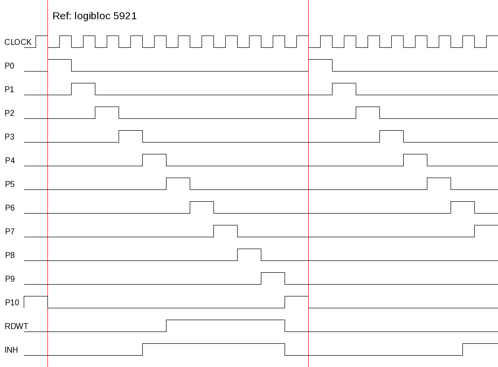
The following table outlines various calculator actions relative to timing signals.
| Phase | Actions |
|---|---|
| P0-P3 | Microcode instruction sense and latch |
| P4 | Latch L,M,N (MOP) |
| P5 | Perform Tape Functions (MOP) |
| P5-P6 | Latch Output Data (MOP) |
| P8 | Latch Q (MOP) |
| Latch next ucode address (JAD/JH/JL) | |
| Clear OFL (JH) | |
| P9 | Latch ALU Output (ZO) |
| Latch SC (AOP) | |
| P10 | Latch S Data (ST) |
| Read/Write memory (MOP) |
| Bits | 42 | 41 | 40 | 39 | 38 | 37 | 36 | 35 | 34 | 33 | 32 | 31 | 30 | 29 | 28 | 27 | 26 | 25 | 24 | 23 | 22 | 21 | 20 | 19 | 18 | 17 | 16 | 15 | 14 | 13 | 12 | 11 | 10 | 9 | 8 | 7 | 6 | 5 | 4 | 3 | 2 | 1 | 0 | - |
|---|---|---|---|---|---|---|---|---|---|---|---|---|---|---|---|---|---|---|---|---|---|---|---|---|---|---|---|---|---|---|---|---|---|---|---|---|---|---|---|---|---|---|---|---|
| Fields | AI | BI | ZO | AOP | AC | BC | Bd | MOP | KK | ST | JAD | JH | JL | - | ||||||||||||||||||||||||||||||
The instruction fields have the following effects on the hardware.
The notation REG<n> refers to Bit "n" of register "REG".
| KK | |
|---|---|
| XXXX | Immediate operand |
|
|
| |||||||||||||||||||||||||||||||||||||||||||||||
|
| ||||||||||||||||||||||||||||||||||||||||||||||||||||||||||||||||||||||||||||
| AOP ALU Function | ||
|---|---|---|
| op | flags updated | Operation |
| 000 | Zbus = Abus + Bbus | |
| 001 | Zbus = Abus + Bbus + 1 | |
| 010 | SC | Zbus = Abus + Bbus |
| 011 | SC | Zbus = Abus + Bbus + SC |
| 100 | SC | Zbus = Abus + Bbus + 1 |
| 101 | Zbus = Abus & Bbus | |
| 110 | Zbus = Abus ^ Bbus | |
| 111 | SC | Zbus = (Abus + Bbus) >> 1 * |
| ALU is always updated. CC is always updated, but based on sum. | ||
* Sum is rotated right thru SC:
Zbus2 = (Abus + Bbus)3 Zbus1 = (Abus + Bbus)2 Zbus0 = (Abus + Bbus)1 SC = (Abus + Bbus)0 | ||
|
|
|
| ||||||||||||||||||||||||||||||||||||||||||||||||||||||||||||||||||||||||||||||||
| |||||||||||||||||||||||||||||||||||||||||||||||||||||||||||||||||||||||||||||||||||
| D | |||
|---|---|---|---|
| 3 | 2 | 1 | 0 |
| STEP | Learn/ Learn and Print |
List/ Learn and Print |
n/a |
| KA | KB | ||||||||
|---|---|---|---|---|---|---|---|---|---|
| 3 | 2 | 1 | 0 | 3 | 2 | 1 | 0 | ||
| MOP == 1010 | In | n/a | n/a | DOT | |||||
| MOP == 1011 | Out | n/a | n/a | DIN | |||||
| MOP == 0110 | In | n/a | n/a | RBS | |||||
| JL == 110 (?) | In | Key/Periph Hi | Key/Periph Lo | ||||||
The calculator memory was based on magnetic core memory technology. This means that reading memory is a destructive operation, clearing the location to all zero. This is used by the microcode in places to clear memory (registers) quickly, but most of the time the microcode must follow any memory read with a memory write in order to restore the contents.
All memory in the calculator is organized as 8-bit words. Memory addresses are byte-addresses, but the calculator interlaces the memory usage by upper (i.e. RA) and lower (i.e. RB) nibbles. Even numbered registers use the upper part of a range of 16 bytes, odd registers use the lower part. Program steps are not interlaced.
The fact that odd/even registers are interlaced in the same bytes of memory means that most of the time the microcode must follow a memory read with a memory write, even if a register is being cleared since only one nibble of the byte is being cleared and the other must be preserved.
| Memory Usage (Model 720C) | ||||
|---|---|---|---|---|
| RAM Address | Registers | Purpose | ||
| Upper | Lower | Upper | Lower | |
| 0x7ff - 0x7f0 | n/a | n/a | Display Register Y | Display Register X |
| 0x7ef - 0x7e0 | n/a | n/a | Temp | Temp |
| 0x7df - 0x7d0 | n/a | n/a | System State | Learn Mode Display |
| 0x7cf - 0x7c0 | 248 (14 08*) | n/a | unknown | Program Stack |
| 0x7bf - 0x7b0 | 246 (14 06*) | 247 (14 07*) | Steps 0000 - 0015 | |
| 0x7af - 0x7a0 | 244 (14 04*) | 245 (14 05*) | Steps 0016 - 0031 | |
| 0x79f - 0x790 | 242 (14 02*) | 243 (14 03*) | Steps 0032 - 0047 | |
| ... etc ... | ||||
| 0x64f - 0x640 | 200 (10 00*) | 201 (10 01*) | Steps 0368 - 0383 | |
| 0x63f - 0x630 | 198 (09 08*) | 199 (09 09*) | Steps 0384 - 0399 | |
| 0x62f - 0x620 | 196 (09 06*) | 197 (09 07*) | Steps 0400 - 0415 | |
| ... etc ... | ||||
| 0x32f - 0x320 | 100 (00 00*) | 101 (00 01*) | Steps 1168 - 1183 | |
| 0x31f - 0x310 | 98 (09 08) | 99 (09 09) | Steps 1184 - 1199 | |
| 0x30f - 0x300 | 96 (09 06) | 97 (09 07) | Steps 1200 - 1215 | |
| ... etc ... | ||||
| 0x02f - 0x020 | 4 (00 04) | 5 (00 05) | Steps 1936 - 1951 | |
| 0x01f - 0x010 | 2 (00 02) | 3 (00 03) | Steps 1952 - 1967 | |
| 0x00f - 0x000 | 0 (00 00) | 1 (00 01) | Steps 1968 - 1983 | |
| * Access directly only by "direct +100" function codes | ||||
Editor's Note: It is not known whether the 249th register (0x7cf - 0x7c0 upper) is an anomaly of the microcode or actually intended as a register. T.B.D. whether that memory gets used by the microcode for something else (e.g. temporary storage during certain operations).
The Program Stack is organized as five 12-bit values stored big-endian, with the low 11 bits being the memory address of the the program step that made the call (i.e. return must decrement this address for the next program code to execute) and the high bit is a flag indicating the mode which called the subroutine: 1 = Keyboard (stopped), 0 = Running Program. Address 0x7c0 lower is the high 4 bits of the "top of stack". Each time the stack is "pushed" the entire contents is copied/shifted right. When the stack is "popped" it is copied left. The stack is not guarded against overflow, with entries being pushed off the end and lost.
| System State (0x7df - 0x7d0 upper, 0x7cf lower) | |
|---|---|
| 0x7cf | DIR+100 (08) |
| 0x7d0 | P.C. Hi |
| 0x7d1 | P.C. Med |
| 0x7d2 | P.C. Lo |
| 0x7d3 | Prefix State |
| 0x7d4 | |
| 0x7d5 | Number Entry State |
| 0x7d6 | Low nibble of direct command (if Prefix State is 08) |
| 0x7d7 | Low nibble of WRITE command (if Prefix State is 04) |
| 0x7d8 | Extended Math State |
| 0x7d9 | |
| 0x7da | other state 10 |
| 0x7db | |
| 0x7dc | |
| 0x7dd | other state 13 |
| 0x7de | |
| 0x7df | |
| 00 = no prefix |
| 04 = WRITE, MARK |
| 08 = Direct (incl 12 xx) |
| 12 = SEARCH |
| 01 = Running (OR'ed with above) |
| 08 = Direct+100 (any 12 xx prefix) |
| 00 = no entry |
| 01 = mantissa, leading zero |
| 02 = mantissa, non-zero |
| 03 = exponent |
| 04 = decimal, non-zero |
| 05 = decimal, leading zero |
| 06 = Set P.C. |
| 3 | 2 | 1 | 0 | ||||
|---|---|---|---|---|---|---|---|
| Sign | ? | Quadrant
| |||||
| 3 | 2 | 1 | 0 |
|---|---|---|---|
| ? | state | ? | ? |
| 3 | 2 | 1 | 0 |
|---|---|---|---|
| ? | state | ? | ? |
The microcode refreshes the display by sequentially loading each digit from memory, and pausing for about 431 cycles (almost 593 uS). This means the entire display (16 digits) is refreshed every 9.5 mS, or about 105 times a second. The display decoders are fed directly from the output latch of RAM (RA,RB) and the N address register. N contains the column (digit) number to enable, and the RAM latch contains the code for the digit to be displayed, and both must be kept static during the pause.
The displays do not consume a digit column for the decimal point. This means that the calculator must provide addition data to the display hardware. The machine state register (S) is used to select "fixed" or "floating" decimal for the X and Y displays, seaprately. When fixed decimal, the decimal point in column 0 is on. When floating decimal, the last three columns (exponent) are blank so the display expects column 15 refresh data to contain the decimal point position. This means that the decimal point is actually display after all the digits are displayed.
The display decodes digit values differently depending on the column. Column 0 is a "sign/dp" digit and will only display "+", "-", "." and blank. Column 13 is a "sign-only digit and will only display "+", "-", and blank. The decimal point does not consume a column, but is displayed either fixed on column 0 (for scientific notation) or for floating point, when columns 13, 14, and 15 are always blank, the hardware uses the value of the "digit" in column 15 as the decimal point selector. Both X and Y displays are refreshed simultaniously, and both independently select fixed or floating decimal point. The machine state register holds the bits (during refresh) for selecting fixed/floating for both X and Y displays.
The following are provided by the calculator during refresh:
| S | RA | RB | N | ||||||||||||
|---|---|---|---|---|---|---|---|---|---|---|---|---|---|---|---|
| 3 | 2 | 1 | 0 | 3 | 2 | 1 | 0 | 3 | 2 | 1 | 0 | 3 | 2 | 1 | 0 |
| n/a | FXDX | FXDY | Y digit | X digit | Column | ||||||||||
The display hardware decodes the register contents without modification, other
than selecting fixed or floating point. The display pattern is the same as
the register pattern. This means the calculator does not need
to keep a "formatted" copy of each display, it directly refreshes the
actual register contents.
Cassette Tape
Most cassette storage of the era used audio modulation, similar to the "musical tones" of a modem, and used standard audio cassette tapes. But the Wang 700 used magnetic saturation like mainframe computer tape drives. It did work on audio cassettes, but Wang recommended high quality "metal" tape.
Because magnetic media only works when there are changes in magnetic fields, the encoding had to ensure that the magnetic field changed frequently. This means that, for example, a long string of zeroes must not result in a long period of blank tape. The data encoding used a clock with data pulse between each clock. A parity bit was added every 8 data bits, to help detect errors.
The timing of each bit was precise, because the tape read code had to be able to stay synchronized without saving state information or doing much processing. Each unit of output was 385 cycles (data bit width 1550), and each program (tape image) was preceded by a 524,290 cycle (approximately 0.67 second) blank gap (no magnetic field transitions).
During read, the calculator waits for the "bit start" transition, then delays 962 cycles before sampling again. If the sample reveals that there was a "1" pulse, then the bit is considered a "1", otherwise it is "0". From this stream, the calculator assembles bytes and checks parity, loading data into memory.
Here is an example of writing 09 00 to tape and reading it back:
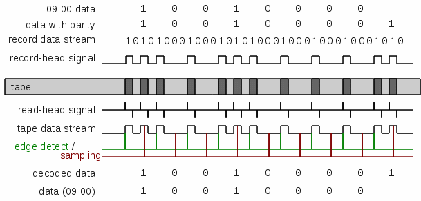
The code 09 00 is encoded bit by bit, and an odd parity bit added after. Each bit is encoded into the tape stream by converting "1" into "1010" and "0" into "1000". There is effectively a clock always present with optional data bit pulse between any two adjacent clock pulses. The resulting stream is fed to the record head and produces alternating segments of positive and negative magnetic fields on the tape.
During read, the changes between positive and negative magnetic fields show up as "blips" in the signal from the tape read head. The positive blips and negative blips are fed through a transister "one-shot" that effectively reproduces the original record head data stream.
The calculator monitors the signal from the one-shot. The first "1" it sees indicates the beginning of a clock pulse. It then delays 962 cycles and checks the signal again. If it is still "1" (was actually re-triggered by a second pulse) then the data bit is interpreted to be a "1". Otherwise, the data bit is interpreted to be "0". These bits are assembled into an 8-bit word and a parity bit, which is then checked for odd parity and, if correct, the data word is stored in memory.
A parity error will cause the calculator to turn on the Mach Error flag (ERR) and stop processing the tape.
Other problems with the tape will generally cause the calculator to "hang" with a blank display. Pressing PRIME is usually required in order to recover.
The calculator reads/writes the tape at about 519 bits/second. Assuming standard
tape speed, this makes a tape density of a little less than 300 bpi
(compare to mainframe "9-track" tapes which were 800 or 1600 bpi, and later 6250 bpi).
The smallest common audio cassette was 15 minutes (C15) which would hold an
overwhelming 50,000 program steps (on both sides) or
26 complete copies of the calculator memory (a program rarely consumed all of memory).
For this reason, Wang data cassettes were much shorter,
typically only having a few minutes of tape.
Expansion (Peripheral) Ports
Note: Assumtion at this point is that the Wang 700 pripherals operated identically to the Wang 600. The following is from the Wang 600:
| GIOB<0:3> | GIOA<0:1> | ostb | AK(i) | n/c | gnd | pwr | |||||
| 1 | 2 | 3 | 4 | 5 | 6 | 7 | 8 | 9 | 10 | 11 | 12 |
|---|---|---|---|---|---|---|---|---|---|---|---|
| 13 | 14 | 15 | 16 | 17 | 18 | 19 | 20 | 21 | 22 | 23 | 24 |
| gnd | n/c | chass | gnd | ||||||||
Signals with (i) are inputs to the calculator, all others are outputs.
Programming:
| WRITE ALPHA |
character data... (00-00 thru 07-15) |
END ALPHA |
Each character is output on CN-24 with IOB set to 001. Character data codes are described in Character Codes. Note that codes 04-00 thru 07-15 are plotting variations of codes 00-00 thru 03-15 (when device supports plotting).
Additional two-step codes output formatted numbers or fields of spaces.
| DH<0:3>(i) | DL<0:3>(i) | istb(i) | PRIME(i) | Learn(i) | AL<0:3> | D<0:2> | |||||||||||
| 1 | 2 | 3 | 4 | 5 | 6 | 7 | 8 | 9 | 10 | 11 | 12 | 13 | 14 | 15 | 16 | 17 | 18 |
|---|---|---|---|---|---|---|---|---|---|---|---|---|---|---|---|---|---|
| 19 | 20 | 21 | 22 | 23 | 24 | 25 | 26 | 27 | 28 | 29 | 30 | 31 | 32 | 33 | 34 | 35 | 36 |
| D<3> | GIOB<0:3> | GIOA<0:3> | IOB<0:2> | ostb | iack | gnd | chass | ||||||||||
Signals with (i) are inputs to the calculator, all others are outputs.
The connector supplies the "always on" signals from AL<0:3> and D<0:3>, which are essentially display refresh data. This supports a device known as "Classroom Display" which was a large-digit remote copy of the main display.
The signals from IOB<0:2> are used to select devices on the daisy-chain. The following codes are used:
| IOB | Device | Command(s) |
|---|---|---|
| 000 | no device | |
| 001 | CN-24 (no device on CN-36) | WRITE ALPHA ... END ALPHA WRITE 00 xx thru 09 xx WRITE 12 xx |
| 01X | Block I/O | 08 xx |
| 100 | Various Peripherals | GROUP 1 xx xx from Keyboard |
| 101 | GROUP 2 xx xx from Keyboard | |
| 110 | GROUP 1 xx xx in Program | |
| 111 | GROUP 2 xx xx in Program | |
These indicate a GROUP 1 or GROUP 2 command, with the GIOA/B outputs showing the device address code (code after the GROUP 1/2). If a device is configured for the address, it activates and remains selected based on the type of device. Some devices only provide input to the calculator, and will de-activate when the GO command terminates input. Other devices (Block I/O devices) auto-send a GO immediately and remain active until a GROUP 1/2 command selects a different device.
The protocol is as follows (GROUP y xx xx command):
Note: The calculator cannot tell the difference between codes sent by device and codes entered from keyboard.
Programming:
* Block I/O devices (below) do not send any input or require user actions.
| IOB | Meaning |
|---|---|
| 010 | Command mode (Calculator to Device) |
| 011 | Data mode (direction depends on command) |
The protocol is as follows (08 xx command):
If the result code is not 00, the calculator sets OFL (Prog Error).
Each byte sent from device is "seen" by the calculator as keyboard input, and is acknowledged by the act of reading that "keyboard code".
Each byte sent from the calculator is acknowledged by the device by sending a dummy "keyboard code".
Programming:
The first step is only required if it was possible that other GROUP I/O devices were used since the desired target device was last activated.
| xx | Size Code | Meaning | xx | Size Code | Meaning | |
|---|---|---|---|---|---|---|
| 00 | 0x01 | Read 1 byte (step) | 08 | 0x81 | Write 1 byte (step) | |
| 01 | 0x02 | Read 8 bytes (steps) | 09 | 0x82 | Write 8 bytes (steps) | |
| 02 | 0x04 | Read 16 bytes (steps) | 10 | 0x84 | Write 16 bytes (steps) | |
| 03 | 0x08 | Read 32 bytes (steps) | 11 | 0x88 | Write 32 bytes (steps) | |
| 04 | 0x10 | Read 64 bytes (steps) | 12 | 0x90 | Write 64 bytes (steps) | |
| 05 | 0x20 | Read 128 bytes (steps) | 13 | 0xa0 | Write 128 bytes (steps) | |
| 06 | 0x40 | Read 256 bytes (steps) | 14 | 0xc0 | Write 256 bytes (steps) | |
| 07 | 0x00 | (nothing) | 15 | 0x80 | (nothing) |
The "Block I/O" (code 08 xx) devices include extended memory, dual cassette, floppy diskette, as well as the Model 730 Fixed/Removable Disk. The protocol is a block input/output of program steps, but could be used for (extended) register data as well. Sufficiently sophisticated code in ROM could allow all of RAM to be used for registers, and/or implement a simple "operating system" that demand-paged program and register data in RAM.